Showing posts with label chips. Show all posts

2012-04-21

Cellphones That Can See Through Walls

Your Next Phone May Be Able to See Through Walls | PCWorld

Researchers at the University of Texas at Dallas disclosed this week that they've developed an imager chip that could turn mobile phones into devices that can see through walls, wood, plastics, paper, and other objects.
[...]
Portions of the electromagnetic spectrum are already used for consumer devices. For example, microwaves are used to cook food, broadcast radio uses AM and FM waves, and infrared waves are used for seeing in the dark. For their purposes, the researchers used waves in the terahertz range.

Team Finds Possibilities in Untapped Terahertz Range - UT Dallas News

Tapping the Terahertz Gap

Shown is the electromagnet spectrum, from radio waves used for FM and AM signals, to infrared waves used for remote controls, to gamma rays that kill cancer cells.  A team at UT Dallas is focusing on the "terahertz band," which has not been accessible for most consumer devices.


Dr. Kenneth O, director of the Texas Analog Center of Excellence and a professor of electrical engineering, left, worked with a team including Dae Yeon Kim, who was among the authors of the research report.

Will Cellphones Be Able to See Through Walls? New Research Says Yes


When signals on the terahertz band travel from your phone, they’ll bounce back — and that’s when the microchip comes in. The chips are manufactured using CMOS (Complementary Metal-Oxide Semiconductor) technology, which is the basis of most of the electronic devices around you. A censor in the chip will pick up terahertz signals and then images can be created.

If terahertz-band signals can create images with fewer lenses — which would be the case with this technology — that means less money for lenses and a smaller camera. By using a CMOS sensor, the cost becomes even cheaper.

“CMOS is affordable and can be used to make lots of chips,” said Dr. O. “The combination of CMOS and terahertz means you could put this chip and receiver on the back of a cellphone, turning it into a device carried in your pocket that can see through objects.”


2010-03-25

Self-assembling Computer Chips

Self-assembling computer chips

Molecules that arrange themselves into predictable patterns on silicon chips could lead to microprocessors with much smaller circuit elements.

The features on computer chips are getting so small that soon the process used to make them, which has hardly changed in the last 50 years, won’t work anymore. One of the alternatives that academic researchers have been exploring is to create tiny circuits using molecules that automatically arrange themselves into useful patterns. In a paper that appeared Monday in Nature Nanotechnology, MIT researchers have taken an important step toward making that approach practical.


MIT researchers coaxed tiny, chainlike molecules to arrange themselves into complex patterns, like this one, on a silicon chip. Previously, self-assembling molecules have required some kind of template on the chip surface — either a trench etched into the chip, or a pattern created through chemical modification. But the MIT technique instead uses sparse silicon “hitching posts.” The molecules attach themselves to the posts and spontaneously assume the desired patterns.
Image: Yeon Sik Jung and Joel Yang


Research Areas:

Prof. Ross’s group research is directed towards the following areas:
  • Fabrication of magnetic films, multilayers and small magnetic structures, with applications in magnetic logic, magnetic random access memory, hard disks, and bit-patterned media
  • Magnetooptical oxides including perovskites and other oxides for use in integrated optical components such as magnetooptical isolators
  • Self-assembly of block copolymers, with particular application to nanolithography, and in other self-assembling systems such as dewetting of thin metal films and porous alumina formation.

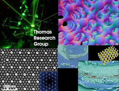
Clipped from: Thomas Research Group


MISSION

Our research is focused on the development of novel polymers and polymer-based composite materials with unusual optical, mechanical, and electronic properties. The research is very interdisciplinary with members having backgrounds in materials science, chemistry, physics and mechanical engineering. The main areas of current interest include photonics, phononics, mechanical properties of complex materials, and polymer structure and morphology.


Molecules could create tiny circuits on computer chips

With its minor reliance on electron-beam lithography, the new method could offer cost-effective fabrication in areas besides . For example, the technique could be used to produce stamps for creating magnetic patterns on hard disks, which are currently produced with electron-beam lithography. However, more research is required before manufacturing individual computer chips with self-assembling molecules, such as getting the molecules to form the exact patterns needed to produce functioning circuits.

More information: Joel K. W. Yang, Yeon Sik Jung, Jae-Byum Chang, R. A. Mickiewicz, A. Alexander-Katz, C. A. Ross & Karl K. Berggren. “Complex self-assembled patterns using sparse commensurate templates with locally varying motifs.” Nature Nanotechnology. Doi:10.1038/nnano.2010.30.
via: MIT News


Sources:
  1. Self-assembling computer chips
  2. Magnetic Materials and Devices Group - MIT
  3. Thomas Research Group
  4. Thomas Group Research
  5. Molecules could create tiny circuits on computer chips
Related:
  1. Building microchips from the bottom up (8/16/2008)
  2. MIT building self-assembling computer chips | Crave - CNET
  3. Microsoft Word - chuang_tsa.doc - Powered by Google Docs
  4. Molecules arrange themselves into predictable patterns
  5. Building microchips from the bottom up
  6. DMSE - Faculty - Caroline A. Ross
  7. Complex self-assembled patterns using sparse commensurate templates with locally varying motifs : Abstract : Nature Nanotechnology

2009-10-02

NVIDIA's Next Generation Chip Architecture 'Fermi'

clipped from www.reuters.com
Reuters

Nvidia pushes further into mainstream computing

The company, which made its name selling specialty computer graphics chips designed for gaming, on Wednesday demonstrated a new chip architecture code-named "Fermi," which Nvidia's Chief Executive Jen-Hsun Huang said will roll out in the next few months across the company's GeForce, Quadro and Tesla graphics processors.

clipped from www.nvidia.com
NVIDIA
The Next Generation CUDA Architecture, Code Named Fermi
The Soul of a Supercomputer in the Body of a GPU
The next generation CUDA architecture, code named “Fermi”, is the most advanced GPU computing architecture ever built. With over three billion transistors and featuring up to 512 CUDA cores, Fermi delivers supercomputing features and performance at 1/10th the cost and 1/20th the power of traditional CPU-only servers.
clipped from www.youtube.com
clipped from www.techtree.com
Logo
The new set new technologies that arrive in Fermi architecture are:

  • C++, complementing existing support for C, Fortran, Java, Python, OpenCL and DirectCompute
  • ECC, a critical requirement for datacenters and supercomputing centers deploying GPUs on a large scale
  • 512 CUDA Cores featuring the new IEEE 754-2008 floating-point standard, surpassing even the most advanced CPUs
  • 8x the peak double precision arithmetic performance over NVIDIA's last generation GPU. Double precision is critical for high-performance computing (HPC) applications such as linear algebra, numerical simulation, and quantum chemistry
  • NVIDIA Paralle DataCache - the world's first true cache hierarchy in a GPU that speeds up algorithms such as physics solvers, raytracing, and sparse matrix multiplication where data addresses are not known beforehand
  • NVIDIA GigaThread Engine with support for concurrent kernel execution, where different kernels of the same application context can execute on the GPU at the same time (eg: PhysX fluid and rigid body solvers)
  • Nexus, the world's first fully integrated heterogeneous computing application development environment within Microsoft Visual Studio

blog it
Sources:
  1. Nvidia pushes further into mainstream computing | Industries | Technology, Media & Telecommunications | Reuters
  2. Next Generation CUDA Architecture, Code Named Fermi
  3. YouTube - Introducing the Next Generate CUDA GPU Architecture, Code Named "Fermi"
  4. Techtree.com India > News > Hardware > Nvidia unveils Fermi GPU Architecture
Related:
  1. Nvidia's 'Fermi' GPU architecture revealed - The Tech Report - Page 1
  2. Nvidia gives first look at next-gen Fermi GPU | Crave - CNET
  3. Nvidia Dives Deeper into Supercomputing with Fermi - Computing News - Digital Trends
  4. Welcome to NVIDIA - World Leader in Visual Computing Technologies
  5. The world’s first teraflop many-core processor

2008-02-26

IBM's self-assembling nanotechnology

Self-assembly is a term used to describe processes in which systems of pre-existing components form an organized structure as a consequence of specific, local interactions among the components themselves, without external direction. IBM is developing ways to use this in the chipmaking process

Helping to keep Moore’s Law alive and well--as shown in recent news--are IBM scientist who have developed a self-assembly technique where microscopic processing structures can develop independently. New York Times author Michael Fitzgerald describes the scientists’ technique:

clipped from www.news.com


Kelly says IBM is developing a number of ways to use self-assembly in other parts of the chipmaking process.


Richard Doherty, director of the engineering consultant group Envisioneering, says self-assembly techniques should also greatly reduce the number of defective chips, helping to give fabs better returns.


The techniques could lead to more dramatic advances. Alain E. Kaloyeros, professor of nanoelectronics at SUNY Albany, says self-assembling nanotechnology will make it possible to etch a computer onto a pair of glasses, or to create "nanobots" that can float in our bloodstreams, searching for cancerous cells that the bots will then eliminate.


blog it
Related:
Reality Crowd » Blog Archive » Moore’s Law and the Future of Computing
Trying to put new zip into Moore's Law | CNET News.com
IBM Press room - Using Self Assembly to Create Airgap Microprocessors - United States
IBM Press room - 2007-05-03 IBM Brings Nature to Computer Chip Manufacturing - United States
IBM Research | Press Resources | IBM demos new nanotechnology method to build chip components
Small Times - IBM's directed self-assembly one facet in broad nanotech program

2008-02-10

Kovio, printing intelligence into everyday products and goods

A new technique, replacing conventional chip-making methods with printing techniques promises low-cost class of electronic paper, displays, labels, RFID tags, sensors, smart cards and perhaps even programmable wallpaper.
The Wall Street Journal Home Page
Kovio, whose backers include widely known venture capitalist Vinod Khosla, says it has developed a kind of silicon ink that can be sprayed on flexible surfaces using commercial printing systems. Where some companies have developed circuit-printing approaches with various organic and inorganic materials, Kovio says it has used its silicon-based process to build unusually fast devices called thin-filmed transistors.
[ The Wall Street Journal ]
Kovio
Inventing breakthrough printed silicon technologies and complete printed system solutions that build intelligence into everyday products and goods, thereby profoundly improving the productivity and profitability of industries including retail, pharmaceutical, consumer electronics, transportation, manufacturing and energy.

Vinod Khosla
:

"Kovio is introducing one of the most disruptive technologies that the electronics and printing markets have seen to date. Its technology offers dramatic cost, resource and energy advantages over traditional silicon. Now for the first time, it is economically feasible to embed intelligence in everyday products thereby transforming the consumer experience."

Technology

Why Print?

Printed silicon electronics combines the intelligence and functionality of silicon semiconductors and the low-cost manufacturing paradigm of graphics printing. Instead of using conventional color inks to print magazines, books and newspapers, this new paradigm uses silicon-based inks to print integrated circuits, sensors and displays. This revolutionary technology brings the value proposition of silicon-based integrated circuits to industries that have until now not been enable to embed integrated circuits in their products.

transbaked
All Printed Silicon TFT

[ Kovio ]


Related:
kovio
Technology Review: Printing Cheap Chips
071123: Printed silicon RF-IDs by Kovio
Log on in EE Times-Asia, keeping ahead of the curve of electronics design
EETimes.com - Printed ICs aim to make mark on mainstream

Blogged with Flock